In this tutorial, we will discuss how to programming GPIO pin to perform I/O functionalities by altering the bits of various GPIO registers of ATtiny3227.
This is part 2 of tutorials for ATtiny3227 AVR programming, focusing on bare metal programming, with ATtiny3227 as the target MCU.
Almost all of embedded programming tutorials started with blinky program. Just like the "Hello World" in c that started somewhat 50-60 years ago since the introduction of C programming. One of the purposes of the the blinky program is to provide a visual clue to show that whatever development board you are using is working, but the princicle of blinking an LED go beyond the toggling of an LED. It demonstrate part of the feature and functionality of General Purpuse I/O (GPIO) of the MCU, even though the first thing you need to learn about embedded programming often not necesssary started with GPIO.
The blinky code often use to show how abstract the development framework is where you could control a GPIO without knowing much of the internal configuration and setup. Take Arduino as an example, Arduino demostrated that you only need a few line of highly-abstraceted code to blink an LED. This often gives beginners an impression that if you could blink an LED, you could then program an Arduino without learning much about the fundamental. So many beginners, together with the proliferation of readily-made Arduino libraries/drivers, have a wrong impression that they could just program an Arduino without the need of learning the underneath programming language (which in the case of Arduino, is C++) or the hardware and architecture of the MCU (which in the case of Arduino Uno is ATMega328). But this is not true, embedded programming can't be separated from reading the datasheet of whatever MCU you are working with, otherwise you won't be able to go far, this is the reason that many Arduino users get stuck in copy-and-paste programming, where they copy the code found in the Internet, and when it is not working, they simply don't know what to do next.
GPIO Ports and Pins
Blinking an LED is a very basic function, but it helps in understanding how to achieve some of the very basic functions of the microcontroller. In the nutshell, when we blink an LED, we are configuring an GPIO interface as an OUTPUT, and then alter the state of that GPIO pin on a particular time interval. Further expand from there, a pin get set as input or output is done by setting the GPIO Direction Register, and then assign a value to the pin through GPIO Output register.
ATtiny3227, like most of the MCU, consists of a number of PORTs, those PORTs are configurable as general purpose analog or digital, input or output, which it is why it is called General Purpose Input and Output (GPIO). The PORT peripheral registers control the I/O pins of the device. Each port instance has up to eight I/O pins for most of the 8-bit MCUs. The ports are named PORTA, PORTB, PORTC, etc. All pin functions are configurable individually per pin.
The block diagram below shows the internal structure of one of the 8 pins within a PORT. I added the color and flow direction to show the Analog Input/Output, Digital Input, and Digital Output flow. The DIRn is part of Direction Register which can be used to set the direction (i.e. input or output) of a pin, the blue dotted line shows how the data is written into the OUTn register to control the output of the pin, the green dotted line shows that data can be read from INn register, and the red dotted line is the most simple one as analog input where all the gates and flip-flops are by-passed and data is direct go into the ADC input or coming out from the DAC output.
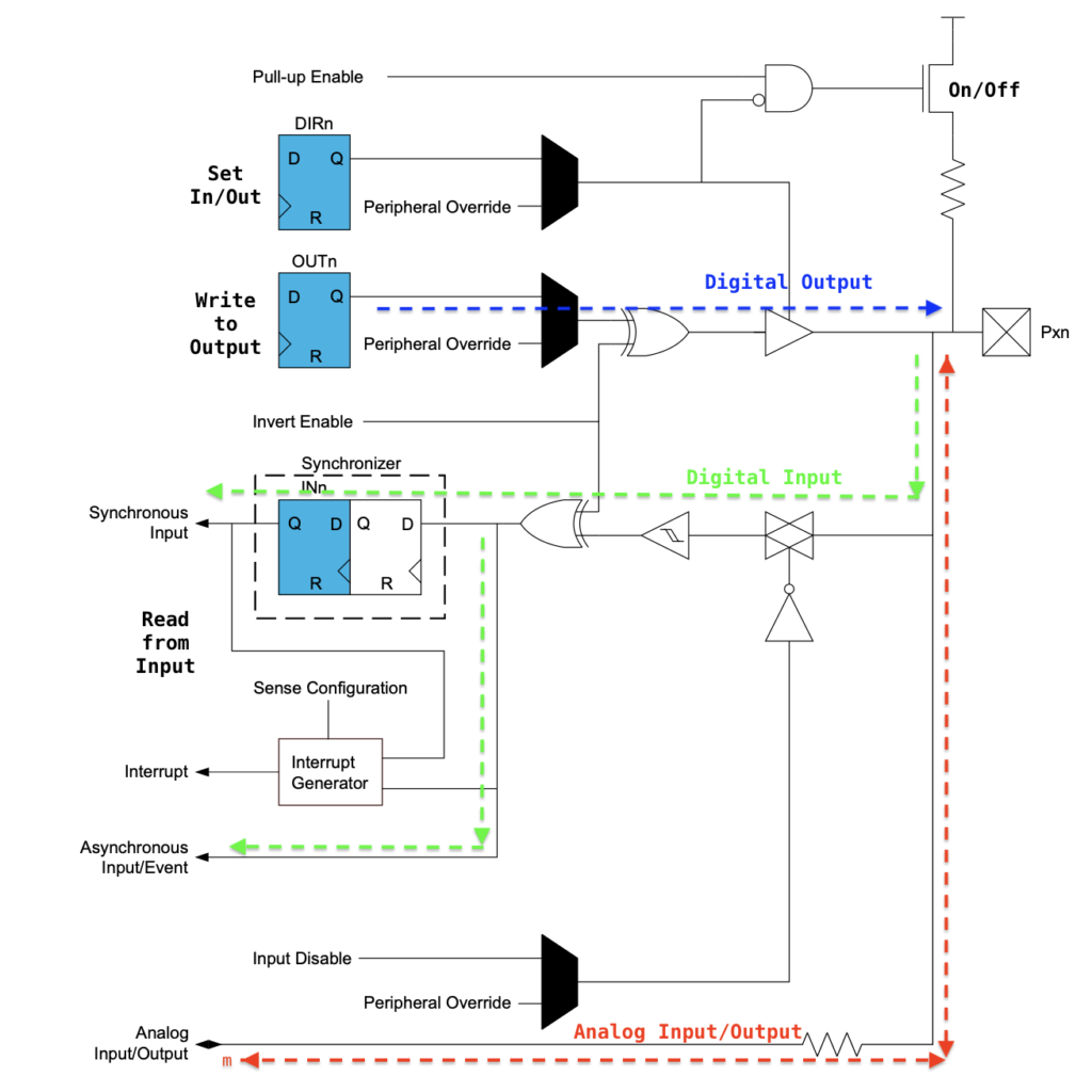
All unused pins, or those used as analog input, or pins used as output can be disabled (through Peripheral Override setting) to reduce the power consumption. Peripherals such as USARTs, ADCs and timers may be connected to I/O pins. When such peripherals is configured, GPIO pin behavior that was normally controlled by PORT can then be overridden by the Peripheral Override.
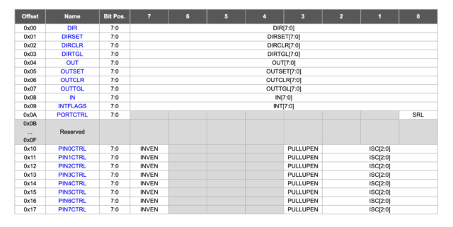
Registers are a critical feature of any microcontroller and are the secret to doing anything with a microcontroller. And a register is essentially just a location within the microcontroller’s address space. The table below shows the register related to GPIO Ports for configuring and controlling the GPIO. We will discuss each of them and demonstrate on how to use those registers.
Among all the registers, there are three important registers:
- The Data Direction Register (DIRn) determines whether the pins operate as inputs or outputs.
- The port output register (OUTn) determines the actual value set on each pin when it’s being used as an output.
- The port input value register (INn) is used for reading input values coming from the outside world.
The AVR-libc has a series of c marcos that defined in the device packs (that we installed before) according the the PORT and name of the register that we need to access to, so this code snippet will set the pin 5 of GPIO PORTA as OUTPUT pin:
PORTA.DIR |= PIN5_bm;PIN5_bm is a macro for bit mask, which means 1 << 5 (shift a 1 to bit 5). The PORTA.DIR |= PIN5_bm is a short form of PORTA.DIR = PORTA.DIR | PIN5_bm, which can further expand to PORTA.DIR = PORTA.DIR | (1 << 5), this can be read in plain English as "read the content of the GPIO.DIR register, bitwise OR it with a 1 shifted to bit position 5, then write it back to GPIO.DIR".
If you have not read the TB3262 AVR1000b: Getting Started with Writing C-Code for AVR® MCUs, we'd suggested that you do so first, it explains in details the coding style and the marco such as
PINx_bmthat we are using throughout this series of tutorials.
To configure a pin as an INPUT, we need to reset the bit related to the pin to 0. This can be done with
PORT.DIR &= ~PIN5_bm;The ~ is a bitwise NOT operator, which turn a 1 to 0 and vice versa, ~PIN5_bm expands to ~(1 << 5) so it shifts a 1 to bit position 5 and NOT 1 is of course a 0.
With the same logic, we can write a data to the OUTn register with:
PORTA.OUT |= PIN5_bm;Reading a value is slightly different, partly because we need to do something with the value we get, as the PORTB.IN gives us the value of all 8 pins, not just the value of the pin that we are looking for. So we invert what we get from the PORTB.IN, then bitwise AND with the bit mask like this:
uint8_t pin2_value = PORTB.IN & PIN2_bm;Please be awared that the pin2_value value is not excatly 0 or 1, it is 0 or 0b00000100 for PIN2 (or 0b10000000 for PIN7), this work fine if all you need is whether the input is a zero or not zero, but if you want to get the true state of the GPIO pin, it need to be shifted down based on its bit position.
uint8_t pin2 = (PORTB.IN & PIN2_bm) >> PIN2_bp; // input is 0 or 1or perform a boolean check to get a 1 if PIN2 is set, or 0 if PIN2 is cleared.
uint8_t pin2 = ((PORTB.In & PIN2_bm) == PIN2_bm); // this return 0 or 1 instead of 0 or b00000100Blinking an LED
With what we learnt so far, we can write our Blinky program to blink the LED. The following program setup GPIO port A pin 7 as OUTPUT, the infinite while(1) loop set the bit 7 (that is, corresponding to Pin 7) to 1, delay by 500 mini-seconds(ms), and then set the pin to 0 with another 500ms delay. The two #include header files are part of the avr-libc for definition of all the io pins for various AVR chips and utility program for the _delay_ms() function.
#include <avr/io.h>
#include <util/delay.h>

int main() {

    _PROTECTED_WRITE(CLKCTRL.MCLKCTRLB, !CLKCTRL_PEN_bm); // disable prescaler to run at 20MHz
    while (!(CLKCTRL.MCLKSTATUS & CLKCTRL_OSC20MS_bm)) {};

    PORTA.DIR |= PIN7_bm;       // Set PA7(LED) as output

    while(1) {
        PORTA.OUT |= PIN7_bm;   // Set PA7 to 1
        _delay_ms(500);
        PORTA.OUT &= ~PIN7_bm;  // Set PA7 to 0
        _delay_ms(500);
    }

    return 0;
}
If you ever program Arduino before, you might noticed that this is quite similar to Arduino's blinky sketch where PORTA.DIR |= PIN7_bm has the same effect as Arduino's pinMode(PIN7, OUTPUT), and PORTA.OUT |= PIN7_bm is similar to digitalWrite(PIN7, HIGH). This is however faster than the Arduino code because we manipulate the register directly without the overhead introduced by the Arduino framework.
Read-Modify-Write or Atomic Operation
So far we set the GPIO pin direction by reading the PORTA.DIR register, performs a bitwise OR of what we read from the register with the pin mask PIN7_bm and then write it back to PORTA.DIR. The bitwise OR ensures that we only change the pin that we want to modify without affecting the rest of pins, this is why we need to read the states of the PORTA.DIR register first to get the states of all the pins first. If we accidentially prform a PORTA.DIR = 0B10000000 by directly write the data to the direction register, we indeed set the bit 7 to 1 (i.e. set PIN7 as OUTPUT), but we also set the rest of the bits to 0 (rest of the PINs as INPUT). The PORTA.DIR |= 0B10000000 prevent us from accidentially set the rest of the pins direction.
This read-modify-write operation, and often requires multiple MCU clock cycles to complete the operation. As you might noticed in the register table that we shown privously, there are several registers that we haven't talk about yet, namely DIRSET (Direction Set), DIRCLR (Direction Clear) and DIRTGL (Direction Toggle) registers for direciton control, OUTSET (Output Set), OUTCLR (Output Clear) and OUTTGL (Output Toggle) registers for output data set, clear and toggle operation.
The different of DIRSET/DIRCLR registers from PORTx.DIR register is that these registers can be used to set/clear the GPIO direction of a particular pin by setting the corresponding bit to '1' with a single (atomic) operation instead of a read-modify-write operation. So it is faster because it use less clock cycle to achieve the same goal. Furthermore, write a '0' to DIRSET/DIRCLR to a particular bit has no effect to the corresponding pin, that is, it won't have the potential side-effect of accidentally set the unrelated pins. Another direction related register is DIRTGL reigster, writing a '1' to bit n in this register will toggle the corresponding bit in PORTx.DIR.
Similarly for OUTSET, OUTCLR and OUTTGL registers.
With these new understanding, we can modified our blinky program to use those registers instead:
#include <avr/io.h>
#include <util/delay.h>

int main() {

    _PROTECTED_WRITE(CLKCTRL.MCLKCTRLB, !CLKCTRL_PEN_bm); // disable prescaler to run at 20MHz
    while (!(CLKCTRL.MCLKSTATUS & CLKCTRL_OSC20MS_bm)) {};

    PORTA.DIRSET = PIN7_bm;       // Set PA7(LED) as output

    while(1) {
        PORTA.OUTSET = PIN7_bm;   // Set PA7 to 1
        _delay_ms(500);
        PORTA.OUTCLR = PIN7_bm;   // Clear PA7 to 0
        _delay_ms(500);
    }

    return 0;
}
We can further simplified our code by replacing the OUTSET and OUTCLR with the OUTTGL register.
#include <avr/io.h>
#include <util/delay.h>

int main() {

    _PROTECTED_WRITE(CLKCTRL.MCLKCTRLB, !CLKCTRL_PEN_bm); // disable prescaler to run at 20MHz
    while (!(CLKCTRL.MCLKSTATUS & CLKCTRL_OSC20MS_bm)) {};

    PORTA.DIRSET = PIN7_bm;       // Set PA7(LED) as output

    while(1) {
        PORTA.OUTTGL = PIN7_bm;   // Toggle PA7(LED)
        _delay_ms(500);
    }

    return 0;
}
How about Button Input?
We can't talk about GPIO without mentioning button, button in a way is an input device where we could connect to a GPIO pin and detect its state, pressed or not pressed. We briefly mentiond about the PORTx.IN register and about reading the the value of the PORTx.In previously. If we connect a button between GND and a GPIO pin, the status of the GPIO pin, when configures as an INPUT, is neither 1 nor 0, meaning the input stage is in a floating state, so we need to have a pull-up resistor pull the pin to the VCC level (3.3v or 5V depend the MCU supply voltage), then the GPIO pin would be at HIGH when the button is not pressed, and when the button is pressed, it bring the voltage at the pin to GND. As you can see from the block diagram of GPIO pin, internally there is a pull-up resistor that can be programmably turn on or turn off. This internal pull-up resistor is controlled by PINnCTRL register.
In the following program the LED will be off when the program started, press the button that connected to the PA0 will turn it on, and press the button again will turn off. Noticed that the datasheet showing that when an MCU is power-up, by default the PORTx.DIR has a default value of 0, meaning that all the pins are in INPUT mode by default, therefore PORTA.DIRCLR = PIN0_bm is not necessary, but explicitly clear the pin making the intension more clear. PORTA.PIN0CTRL = PORT_PULLUPEN_bm enables the pull-up resistor on Pin 0.
#include <avr/io.h>
#include <util/delay.h>

int main() {

    _PROTECTED_WRITE(CLKCTRL.MCLKCTRLB, !CLKCTRL_PEN_bm); // disable prescaler to run at 20MHz
    while (!(CLKCTRL.MCLKSTATUS & CLKCTRL_OSC20MS_bm)) {};

    PORTA.DIRSET = PIN7_bm;               // Set PA7(LED) as output

    PORTA.DIRCLR = PIN0_bm;               // Set PA0 to input
    PORTA.PIN0CTRL = PORT_PULLUPEN_bm;    // Enable PA0 PULLUP

    while(1) {

        if ((PORTA.IN & PIN0_bm) == 0)
            PORTA.OUTTGL = PIN7_bm;

    }

    return 0;
}
Button Debounce
You will noticed that the program that we just shown you is not working reliably, sometime when the LED is supposed to be turn off, it stays on, or vice versa.
This is because that button is an electronic device with mechanical parts, the contacts inside the button bouncing around in the first a few microseconds (sometime even a few milliseconds) or so like a spring, when the MCU running in the while(1) at high speed (our MCU is running at 20MHz), it would be able to detect those bounce activities, like someone is flipping a light switch rapidly, as the result, the state of the button is switching between HIGH and LOW several times before it settled to the state that it supposed to be.
There are both hardware and software solutions for solving such problem, hardware solution requires extra resistors and capacitor and take up PCB space, and requires planning during the design stage of the circuit design, but if you want to have any GPIO to be configured as a button input during software development, a software debounce solution is the way to go.
The following code consists of a debounce function that can be used by any GPIO PORT and PIN.
#include <avr/io.h>
#include <util/delay.h>

uint8_t debounce(PORT_t * port, uint8_t pin_mask) {
  static uint16_t state = 0;

  uint8_t pinState = ((port->IN & pin_mask) == pin_mask);  // pin state as either 0 or 1

  state = (state<<1) | pinState;
  return (state == 0x8000);      // consider debounced if 15 consective LOW are received
}

int main() {

    _PROTECTED_WRITE(CLKCTRL.MCLKCTRLB, !CLKCTRL_PEN_bm); // disable prescaler to run at 20MHz
    while (!(CLKCTRL.MCLKSTATUS & CLKCTRL_OSC20MS_bm)) {};

    PORTA.DIRSET = PIN7_bm;               // Set PA7(LED) as output

    PORTA.DIRCLR = PIN0_bm;               // Set PA0 to input
    PORTA.PIN0CTRL = PORT_PULLUPEN_bm;    // Enable PA0 PULLUP

    while(1) {

        if (debounce(&PORTA, PIN0_bm)) // debounce() return true when button reached to stable LOW
            PORTA.OUTTGL = PIN7_bm;

    }

    return 0;
}
When the button is pressed, the button pull the GPIO pin to ground and produce a 0. The value is added into the state through the bitwise OR | operator, and shift up through shift << operator each time the button pin is read, the 0x8000 is a bit mask that mask-out the MSB, and sort of saying we only care for a pattern that consists of 15-bits consecutive stream of 0.
When you think of the bouncing problem, the button is in an unstable mode for the initial a few microseconds when it is pressed, and could produce a stream of either LOW or HIGH during that period. The debounce function is designed to detect the last transition of the falling edge when the button state transit from the last falling edge (from HIGH to LOW) followed by a pattern consists of a stream of 15-bits of stable LOW state, the statement state | 0x8000 would only be true if the data stream is 1000000000000000 (i.e. 1 was the last bouncing, following by 15 consective read of stable 0), in another word, the button has reached to a stable state and no longer bouncing around.
if you find the debounce code is still occasionally failed to produce the correct button-pressed result, you could introduce a slight delay with _delay_us(5) in the debounce function so that each checking of the button debounce status is now 5us apart, so we are seeking for a reading of 15 consecutive 0 within a window of at least 15x5=75us. You can adjust the value of delay according to the situation as the hardness of the button mechanic part varies.
References
TB3229 - Getting Started with General Purpose Input/Output(GPIO)
A Guide to Debounce by Jack Ganssle